- 您现在的位置:买卖IC网 > Sheet目录1201 > CDB5467U (Cirrus Logic Inc)BOARD EVAL FOR CS5467 ADC
�� �
�
�CS5467�
�9.1.2� Gain� Calibration�
�During� gain� calibration,� a� full-scale� reference� signal�
�must� be� applied� to� the� meter� or� optionally,� scaled� to� the�
�VIN1� ???� VIN2� ??� ,� ?� IIN1� ?� (IIN2� ???� pins� of� the� CS5467.� A� DC�
�reference� must� be� used� for� DC� gain� calibration.� Either�
�an� AC� or� DC� reference� can� be� used� for� RMS� AC� calibra-�
�tions.� If� DC� is� used,� the� associated� high-pass� filter�
�(HPF)� must� be� off.�
��External�
�Connections�
�During� AC� gain� calibration� the� RMS� level� of� the� applied�
�reference� is� measured� with� the� preset� gain,� then� divided�
�into� 0.6� and� the� quotient� stored� back� into� the� corre-�
�sponding� gain� register.�
�9.1.2.2� DC� Gain� Calibration�
�With� a� DC� reference� applied,� the� DC� Gain� Calibration�
�command� measures� and� averages� DC� values� read� on�
�the� specified� voltage� or� current� channels� and� stores� the�
�reciprocal� result� in� the� associated� gain� registers,� con-�
�verting� measured� voltage� into� needed� gain.� Subse-�
�quent� conversions� will� use� the� new� gain� value.�
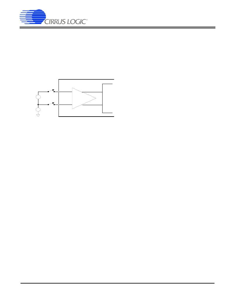
�-�
�-�
�R� eference�
�Signal�
�CM�
�+�
�+�
�IN+�
�IN-�
�+�
�-�
�XG� AIN�
�+�
�-�
�9.1.3� Calibration� Order�
�1.� DC� offset.�
�2.� DC� or� AC� gain.�
�3.� AC� offset� (if� needed).�
�If� both� AC� gain� and� offset� calibrations� were� performed,�
�Figure� 12.� System� Calibration� of� Gain.�
�Using� a� reference� that� is� too� large� or� too� small� can�
�cause� an� over-range� condition� during� calibration.� Either�
�condition� can� set� Status� register� bits� I1OR� (I2OR)�
�V1OR� (V2OR)� for� DC� and� I1ROR� (I2ROR)� V1ROR�
�(V2ROR)� for� AC� calibration.�
�Full� scale� (FS)� for� the� voltage� input� is� ±250� mV� peak�
�and� for� the� current� inputs� is� ±250� mV� or� ±50� mV� peak�
�depending� on� selected� gain� range.� The� normal� peak�
�voltage� applied� to� these� pins� should� not� exceed� these�
�levels� during� calibration� or� normal� operation.�
�The� range� of� the� gain� registers� limits� the� gain� calibration�
�range� and� subsequently� the� range� of� the� reference� level�
�that� can� be� applied.� The� reference� should� not� exceed�
�FS� or� be� lower� than� FS/4.�
�9.1.2.1� AC� Gain� Calibration�
�Full� scale� for� AC� RMS� gain� calibrations� is� 60%� of� the� in-�
�put’s� full-scale� range,� which� is� either� 250� mV� or� 50� mV�
�depending� on� the� gain� range� selected.� That’s� 150� mV� or�
�30� mV,� again� depending� on� range.� So� the� normal� refer-�
�ence� input� level� should� be� either� 150� or� 30� mV� RMS� ,� AC�
�or� DC.�
�Prior� to� executing� an� AC� Gain� Calibration� command,�
�gain� registers� for� any� channel� to� be� calibrated� should� be�
�set� to� 1.0� if� the� reference� level� mentioned� above� is�
�used,� or� to� that� level� divided� by� the� actual� reference� lev-�
�el� used.�
�DS714F3�
�it� is� possible� to� repeat� both� to� obtain� additional� accuracy�
�as� AC� gain� and� offset� may� interact.�
�9.1.4� Temperature� Sensor� Calibration�
�Temperature� sensor� calibration� involves� the� adjustment�
�of� two� parameters� -� ?� V� BE� and� V� BE� 0.� These� values� must�
�be� known� in� order� to� calibrate� the� temperature� sensor.�
��22� for� an� explanation� of� ?� V� BE� and� V� BE� 0� and� how� to� cal-�
�culate� T� GAIN� and� T� OFF� register� values� from� them.�
�9.1.4.1� Temperature� Offset� Calibration�
�Offset� calibration� can� be� done� at� any� temperature,� but�
�should� be� done� mid-scale� if� any� gain� error� exists.�
�Subtract� the� measured� T� register� temperature� from� the�
�actual� temperature� to� determine� the� offset� error.� Multi-�
�ply� this� error� by� ?� V� BE� and� add� it� to� V� BE� 0� to� yield� a� new�
�V� BE� 0� value.� Recalculate� T� OFF� using� this� new� value� .�
�9.1.4.2� Temperature� Gain� Calibration�
�Two� temperature� points� far� enough� apart� to� give� rea-�
�sonable� accuracy,� for� example� 25°C� and� 85°C,� are� re-�
�quired� to� calibrate� temperature� gain.�
�Divide� the� actual� temperature� difference� by� the� mea-�
�sured� (� T� register)� difference� for� the� two� temperatures.�
�This� gives� a� gain� correction� factor.� Update� the� T� GAIN�
�register� by� multiplying� it’s� value� by� this� correction� factor.�
�Update� ?� V� BE� by� dividing� its� old� value� by� the� gain� cor-�
�rection� factor.� It� will� be� needed� for� subsequent� offset�
�calibrations.�
�41�
�发布紧急采购,3分钟左右您将得到回复。
相关PDF资料
CDB5560-2
DEV BOARD FOR CS5560 W/SE INPUT
CDB5571-2
DEV BOARD FOR CS5571 W/SE INPUT
CDB8422
BOARD EVAL FOR CS8422 RCVR
CDB8952T
BOARD EVAL FOR CS8952
CDCE906-706PERFEVM
EVAL MOD PERFORMANCE CDCE906/706
CEVAL-033
BOARD EVAL FOR CVCO33 .3"X.3"
CF37S
COVER FLANGE 37POS FEMALE
CG0402MLC-05LG
SUPPRESSOR ESD 5VDC 0402 SMD
相关代理商/技术参数
CDB5471
制造商:Cirrus Logic 功能描述:Tools Development kit Kit Con
CDB5480U-Z
功能描述:电源管理IC开发工具 CS5480 Eval Board
RoHS:否 制造商:Maxim Integrated 产品:Evaluation Kits 类型:Battery Management 工具用于评估:MAX17710GB 输入电压: 输出电压:1.8 V
CDB5484U-Z
功能描述:电源管理IC开发工具 CS5484 Eval Board
RoHS:否 制造商:Maxim Integrated 产品:Evaluation Kits 类型:Battery Management 工具用于评估:MAX17710GB 输入电压: 输出电压:1.8 V
CDB5490U-Z
功能描述:电源管理IC开发工具 CS5490 Eval Board
RoHS:否 制造商:Maxim Integrated 产品:Evaluation Kits 类型:Battery Management 工具用于评估:MAX17710GB 输入电压: 输出电压:1.8 V
CDB5501
制造商:Cirrus Logic 功能描述:EVAL BOARD FOR CS5501 - Bulk
CDB5503
制造商:Cirrus Logic 功能描述:EVAL BOARD FOR CS5503 - Bulk
CDB5504
制造商:CIRRUS 制造商全称:Cirrus Logic 功能描述:Low Power, 20-Bit A/D Converter
CDB5505
制造商:Cirrus Logic 功能描述:EVAL BD FOR CS5505 - Bulk